D2DB-PM Application
Take line monitoring to the next level with Die-to-Database Pattern Monitor.
View More
D2DB-Image Explorer Toolkit
Create custom solutions by integrating Anchor's powerful vendor-neutral image processing technology.
View More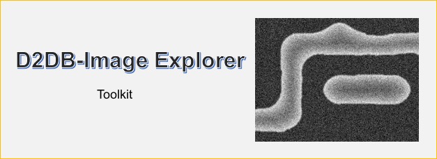
Pattern Centric Yield Manager Application

Pattern Centric Machine Learning Toolkit

More Products Toolkit

Applications

News
Markdown
Writing in Markdown format is a simple and fast way to add styled text to your web pages.
- Ordered and Unordered Lists.
- Simple Links: Stacks can use Markdown Syntax too.
- Simple formatting: Bold and Italic.
- Code snippets:
10 PRINT "HELLO WORLD"
Markdown
Writing in Markdown format is a simple and fast way to add styled text to your web pages.
- Ordered and Unordered Lists.
- Simple Links: Stacks can use Markdown Syntax too.
- Simple formatting: Bold and Italic.
- Code snippets:
10 PRINT "HELLO WORLD"
-
open_in_new{{ post.title }}{{ Feed.sanitiseDate(post.pubDate) }}
{{post.title}}
{{ Feed.sanitiseContent(post.description) }}
Latest Papers


Net Tracing and Classification Analysis on E-Beam Die-to-Database Inspection.
Abstract Only. Please Contact Us for full transcript.
SPIE Vol. 9778 (2016)


Design Guided Data Analysis for Summarizing Systematic Pattern Defects and Process Window.
Abstract Only. Please Contact Us for full transcript.
SPIE Vol. 9778 (2016)


Automatic High Accurate and Efficient Photomask Defects Management Solution for Advanced Lithography Manufacture.
SPIE Vol. 9050-62 (2014)
Featured Product
D2DB Pattern Monitor
Take line monitoring to the next level with Die-to-Database Pattern Monitor. Tap the full potential of SEM images in ways that redefine production line monitoring for advanced technology nodes.
Read More